By breaking up the system-on-a-chip model, the future of semiconductors is going to look very different from the last two decades.
Since the earliest days of semiconductors, researchers have been working to make transistors smaller and cheaper. Fitting more and more transistors into a smaller area can increase the achievable compute power, lower the cost to compute, or combinations of the two. Over the years, a near-constant drumbeat of innovation has driven extraordinary progress in transistor miniaturization: In the early 1970s, the smallest transistors were about 10 micrometers wide — and in 2021, IBM demonstrated that it’s possible to make these components with critical dimensions measured at just a few nanometers. That’s roughly 1,000 times smaller.
Computer chips today are of course considerably more powerful than they were in the earliest days of the personal computer and benefit enormously from the increased transistor density. In pursuit of more compact and lower-cost systems, a key strategy the industry has pursued was to develop SOCs (or systems on a chip). This is where multiple computing functions are swept up into a single chip, creating more complex systems in a smaller area. A typical SoC would include sub-blocks that enable general-purpose processing, custom accelerators, data storage, and high-speed input and output (I/O) communication. This SOC strategy has been extremely successful in making computing systems more functional and less expensive to produce.
But there are forces at work that are driving the industry to start exploring approaches outside the traditional SOC structure. Moore’s Law has started to slow, but there are many other reasons to design new chips today that would’ve been unimaginable just a few decades ago, from processing big data to supporting computation using massive AI models. Fitting all the function you might want in an SOC could result in a design that’s too costly for the market that you want to address — or what you want to achieve could be more efficiently done through mixing and matching components together, rather than combining several SOCs and other elements in a system. And there are some chip functions that have already achieved their optimum performance for their circuit size: shrinking them any further for inclusion in an SOC either isn’t possible, is too costly — or won’t bring any additional benefits.
This is where chiplets can help.
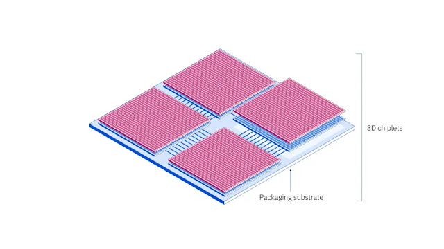
The idea behind chiplets is to break apart the system on a chip into its composite functional blocks, or parts. Sub-elements of a complex-function chip could be made as chiplets, where these sub-elements might include separate computational processor or graphics unit, an AI accelerator, an I/O function, or a host of other chip functions. A system comprised of chiplets is kind of like an SoC on a module, and, in the future, could be made using interoperable mix-and-match chiplet components sourced from multiple providers. This approach could lead to chiplets powering entirely new computing paradigms, creating more energy-efficient systems, shortening system development cycle time, or building purpose-built computers for less than it would cost today.
Why we need chiplets
With increasingly performant chips, computers have continued to unlock even more profound uses. Today, we can use computers to analyze a person’s entire genome in minutes, drive a vehicle remotely, or instantly call up all of the world’s history on our mobile devices.
But processing and acting on all the data generated in the world is not always efficient or as effective as it could be. The potential of AI foundation models and large language models (LLMs) is massive, but they require more compute power to train and run than what we’re used to today — as well as increased memory access. Contemporary AI models, with millions or billions of parameters, require more storage space than could fit on an SOC, but the memory also needs to be quickly accessed to rapidly make inferences. In a chiplet system, it could be entirely possible to have a processing unit, an AI accelerator, and stacks of memory all communicating and sharing data almost as if they were all on the same chip.
Moving memory into a chiplet architecture that stacks it closer to the processor can help tackle bigger AI tasks, but also could have massive environmental benefits as well. More than 50% of power consumed by a computer chip is from moving data horizontally around the chip, according to Huiming Bu, vice president of global semiconductor research and Albany operations at IBM Research. “With chiplets, you can move the memory closer to the processing unit, saving energy,” he added. By some estimates, training an AI model can emit as much carbon as running five cars for their lifetimes. Any energy efficiencies that can be gleaned on a single chiplet module could have huge implications when deployed at the scale of a datacenter.
There are several other potential advantages to the chiplet model. Even when working with bleeding-edge technology, you don’t necessarily need the capabilities of that technology for every function in the system you plan to build. For example, if you were working on a system that needed the highest-performance AI inference processors in the world, but weren’t worried about graphics performance and thought a standard I/O connection would suffice, you could spend your money primarily on the resource you specifically needed, rather than SOCs that might have the power you need, but are costly for components your specific task has no use for.
At scale, when producing chiplets, you can achieve much higher yields from a single production run than you could from larger, more complicated chip architectures, Bu said. For organizations looking to use a lot of a specific type of resource, a chiplet structure could be valuable. It also opens the door for a greater number of smaller companies and research institutions to be able to test out the latest technologies for the same reason: Instead of investing in expensive SOCs, teams could spend their money on just the highest performance chiplets they need, and rely on more commoditized technology for other aspects of their modules or devices.
Chiplets could also help to close some of the gap on who gets access to technology. Traditionally, the newest gadgets and hardware are bought by more affluent countries and their companies first, as they can more easily afford it. With time, or economies of scale, what was once cutting-edge becomes commonplace, and is more affordable for the rest of the world. With a chiplet structure, it could be possible for more locations and industries to access newer technology with lower financial barriers. And given that yields are higher for targeted function within chiplets, it’s possible that there could be smaller facilities that spring up to service new markets for chiplets, potentially expanding equity in chipmaking research and access to newer technology.
How IBM is researching chiplets today
Some chipmakers have started making chiplets out of their own hardware designs for proprietary uses, breaking down their components and scaling them for server or computer products that fit their customers’ specific needs. But it’s still early days for the concept of an open chiplet ecosystem.
To ensure chiplets from different manufacturers work together, the way the devices connect has to be standardized. That means the physical connectivity between chiplets has to be standardized – things like compatible signaling levels, voltages, and data transfer rates – but also the digital compatibility aspects, like the number of lanes in a bus, the coding sublayer for error correction, or even just how two devices know to automatically connect and exchange data.
These industry chiplet standards are still being ironed out, but there are two main contenders: the Universal Chiplet Interconnect Express (UCIe) Consortium, and the descriptively named Bunch of Wires specification from the Open Compute Project. IBM researchers are involved with both initiatives, according to Daniel Friedman, a senior manager in communication circuits and systems research.
But instead of waiting for the specifications to be completely finalized, Friedman said that researchers have started exploring various designs for chiplet I/O based on where the two groups are headed. Whatever standard ends up becoming the industry go-to, each chiplet in the eventual system they’re inserted into needs to act as if they were part of a single SoC — and in an ideal world, would deliver similar levels of latency, data transfer, and reliability as an SOC implementation would. And to ensure that IBM is ready to build chiplets as soon as standards are agreed upon, researchers need to engaged now. Some of the early work now in progress is to figure out signal mapping strategies in the context of potential future chiplet packaging solutions.
There are different ways to tackle heterogenous integration, such as stacking chiplets on top of each other, or connecting them together through a device or package that provides a means to support dense electrical communication between devices. The stacking method, called 3D integration, requires innovations in the way chips are built, in both materials and the design. 3D integration requires through-silicon vias (TSVs), or electrical connections that travel through the silicon of each chiplet to connect it to the one above it. IBM researchers in Albany are developing next-generation technologies to advance this concept in chiplets that could be stacked on top of each other beyond options available today. These integration advancements would provide increased performance, with lower energy consumption in a smaller package compared to traditional SoC solutions. This design approach could be more costly to produce, given the additional complexity of the next-generation of high-bandwidth functional layers of TSVs and multi-chiplet module integration.
Chiplets are what’s next in computing
We’re still in the early days of chiplet research and production, but as standards are solidified, that will change. According to Rama Divakaruni, a Distinguished Engineer in process technology research and fabless interfaces at IBM Research, we’ll likely see all sorts of new computing models designed that just wouldn’t have been possible in the past. New technology almost always unlocks new uses. “Human ingenuity is mind blowing,” Divakaruni said, but for many right now researching the future of computing, “they just don’t have the platform now.”
Source: ibm.com


0 comments:
Post a Comment